
HDI PCBs - High Density Interconnect
HDI PCBs – High Density Interconnect
Over time, PCB technology has evolved with the miniaturization of components and semiconductor packages. HDI (High Density Interconnect) technology has been developed along with these trends.
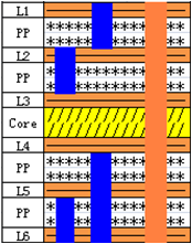
HDI Layer Structure Example
HDI PCBs have a higher circuitry and connection pad density than traditional boards. They are characterized by finer lines and spaces and are made with thin, high-performance materials. They feature microvias, which are smaller than traditional vias, and smaller capture pads.
Boards can be designed to include advanced features such as blind vias, buried vias, via-in-pad, as well as stacked and staggered vias. This gives PCB designers more area to work with. It also allows them to place smaller components closer together. This leads to high-speed, low-loss signal transmission and a board that takes up less space overall.
Manufacturing HDI boards requires special equipment, including laser drills, which are able to achieve drilled diameters typically around 0.006 inches. In addition, laser direct imaging (LDI) is often used, and the board is produced with sequential lamination cycles. For this reason, we have made significant investments in developing our HDI manufacturing technology.
Do you need a quote for high density interconnect boards? Call us toll-free at (852)2797-0355 or submit your design online to receive a fast and accurate quote. To minimize the cost and turn of your PCB order, we recommend you speak with one of our PCB design and manufacturing experts. They can consult with you about the design and specifications of your boards to achieve the capabilities, performance, and cost you are expecting.
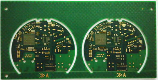
HDI Board Panel